Introduction to Charge Mode Accelerometers

A charge mode accelerometer is a sensor that generates an electrical output proportional to applied acceleration. They are ideal for high temperature vibration applications because they lack internal microelectronics which limits the use of ICP® sensors to about 325 °F. Some charge mode designs can be used up to 1200 °F.

The output of a charge accelerometer is a high impedance charge signal which can be corrupted by cable noise and dirty environmental conditions. It is important to use low noise cables and keep electrical connections as clean as possible. A laboratory style charge amplifier or in-line charge convertor is needed for signal conversion before sending the signal to a data acquisition system or readout device.

A variety of mechanical designs are used to perform the transduction required of charge accelerometers. The designs consist of sensing crystals that are attached to a seismic mass. A preload ring or stud applies a force to the sensing element assembly to make a rigid structure and insure linear behavior. Under acceleration, the seismic mass causes stress on the sensing crystals which results in a proportional electrical output. The output is collected on electrodes and transmitted by wires to an electrical output connector that mates to a low noise transmission cable.

Charge mode accelerometers do not require an external power source like ICP® accelerometers. When mechanical stress is applied, a high impedance charge signal is generated from the piezoelectric sensing element. The high impedance signal requires conversion to a low impedance voltage signal prior to being analyzed by data acquisition or readout devices. The conversion can be done in two ways:

1) With a laboratory style charge amplifier.
2) With an in-line charge convertor and ICP® power source.

Charge amplifiers typically include settings that allow for gain/range adjustment. Other options may include filtering, signal integration and time constant adjustment for low frequency measurements.

In-line charge convertors have a fixed conversion factor (ie – 1 mV/pC or 10 mV/pC) and require power from an ICP® signal conditioner.


Note: Charge convertor selection is dependent upon the operating temperature and insulation resistance of the sensor.

Unlike ICP® sensors, charge sensors are not limited to a maximum 5 volt full scale output range. Charge sensors can operate anywhere within the linear measurement range listed on the specification sheet. The charge output (pC/g) can then be converted by a charge amplifier or charge convertor (mV/pC). Laboratory amplifiers typically have the ability to adjust gain (mV/pC) and measurement range. Charge convertors typically have a fixed gain and measurement range. Example 1 shows a fixed charge gain conversion. Example 2 shows a calculation of system measurement range.

Example 1
Sensor: 357B03, 10 pC/g sensitivity
Charge convertor: 422E52, 10 mV/pC fixed charge conversion
Expected input: 14 g’s

10 pC/g X 10 mV/pC = 100 mV/g X 14 g’s = 1400 mV = 1.4 V

Example 2
Sensor: 357B03, 10 pC/g sensitivity
Charge convertor: 422E52, ±500 pC input range

±500 pC ÷ 10 pC/g = 50 g measurement range

Low frequency and discharge time constant specifications are not included on charge mode accelerometer spec sheets. These are electrical characteristics that are determined by the charge amplifier or in-line charge convertor. Consult the spec sheets of the charge amp or convertor low frequency and time constant information. For example PCB® in-line charge convertor model 422E52 has a time constant of >0.1 seconds and a low frequency response of 5 Hz (-5%).

Every charge mode accelerometer has a natural frequency that will restrict the measurement frequency range to some upper limit. The natural frequency (resonance) is a mechanical characteristic imposed on the accelerometer by its physical design characteristics. Sensitivity rises rapidly as the natural frequency is approached which can often result in an overload of signal output. An example of resonance is show in Figure 5.


It’s important to note that mounting plays a role in obtaining accurate high frequency measurements. Consult installation drawings and product manuals for proper mounting techniques of specific models. Additional information on accelerometer high frequency response and mounting can be found at this link (http://www.pcb.com/Resources/TechnicalInformation/Mounting).

PCB® includes a calibration certificate with every charge accelerometer. This certificate documents the characteristics of each accelerometer and provides exact values for several key specifications. A sample calibration certificate is shown in Figure 6.


Back-to back calibration is performed with the test accelerometer mounted onto a reference accelerometer. This technique provides a quick and easy method for determining the sensitivity of an accelerometer over a wide frequency range.

The reference accelerometer is an extremely accurate device with specifications traceable to a recognized standards laboratory. It is possible to vibrate both accelerometers and compare output data by securely mounting the test accelerometer to the reference standard accelerometer.
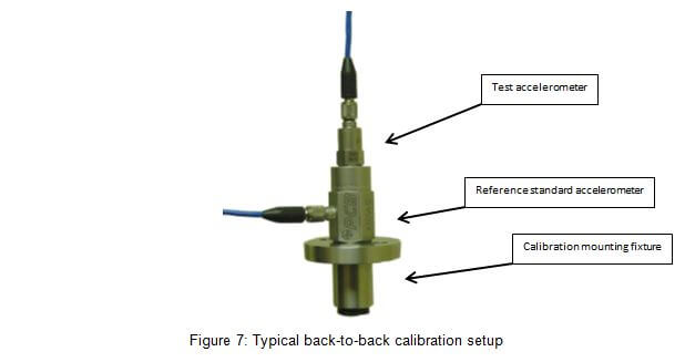


The ratio of the output voltages is also the ratio of the accelerometers’ sensitivities because the acceleration applied to them is the same. The sensitivity of the reference accelerometer is known so the sensitivity of the test accelerometer can be calculated.

Recalibration services are offered for PCB® manufactured accelerometers as well as those produced by other manufacturers. Our internal metrology lab is certified to ISO 9001 and accredited by A2LA. The equipment used during calibration is directly traceable to NIST (National Institute of Standards and Technology).